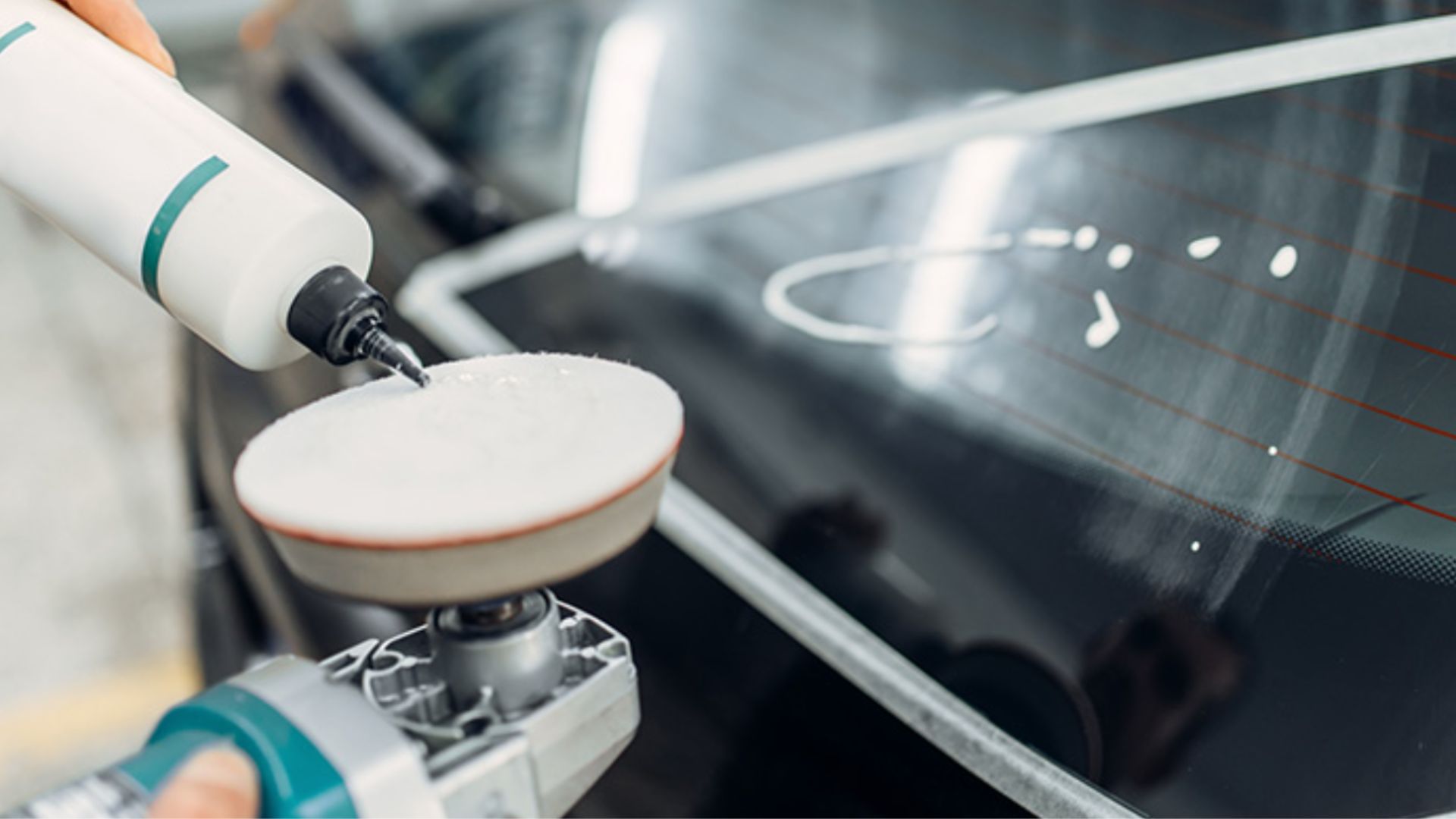
Is a small round tool used for surface polishing and grinding, usually used for repair and care of small areas. In the continuous development of modern technology and manufacturing processes, micro wafers are used as a small but powerful tool in various fields such as automobiles, jewelry, optics and electronics. With their unique properties and wide range of applications, they play an important role in delicate repair and care.
Application and Size
| Industry | Feature | Application | Diameter (mm) | Thickness (mm) |
| Automotive Industry | 1. Paint repair, removal of scratches, stains and oxidation. 2.Realize efficient communication inside the vehicle and between the vehicle and the external environment. | Vehicle sensing, vehicle control, vehicle safety, driver assistance, Internet of Vehicles, intelligent transportation | 1-10 | 0.1-1 |
| Medical Equipment | 1. Real-time monitoring and recording of medical parameters can be realized. 2. Provide portable, wearable and implantable medical solutions. | Miniature wafer sensors, conductive patterns, medical monitoring, medical diagnosis, patient monitoring, biosensing, health management, etc. | 0.2-10 | 0.02-1 |
| Communications Industry | 1. Realize high-speed, high-bandwidth optical communication and radio frequency communication. 2. Provide the functions of optical transmission and radio frequency signal processing. | Microwave optical devices, radio frequency devices, optical transmission, radio frequency signal processing, etc. | 0.1-5 | 0.01-0.5 |
| Consumer Electronics | 1. Provide high-definition, high-color images and display effects. 2. Provide interactive functions of touch and user interface. 3. Adapt to the needs of mobile devices and portable electronic products. | Smartphones, tablets, TVs, touch devices, mobile devices, etc. | 0.5-5 | 0.05-0.5 |
| Electronics Industry | 1. Manufacturing of electronic components, grinding and polishing of semiconductor devices. 2. Can realize high integration and flexible design. | Optical devices, environmental monitoring, medical diagnosis, image sensing, wearable devices, wireless sensing, radar systems, etc. | 0.1-10 | 0.01-1 |
| Jewelry | 1. Restoration and polishing of gemstones and metal surfaces. 2. Generate rich optical effects through the refraction and reflection of light. | Use sparkle and color change to add uniqueness and appeal to jewelry pieces. | 0.5-10 | 0.05-1 |
| Optics | 1. Can control the transmission direction and intensity of light. 2. Adjust the phase and focal length of the optical system to improve imaging quality and resolution. | Optical filters, mirrors, encoders, diffusers, etc. | 0.2-10 | 0.02-1 |
| Metal Processing | 1. High precision processing and excellent wear resistance. 2. High hardness, high strength and high precision processing can ensure the precise forming and high consistency of metal workpieces | 1. As parts of the mold, such as mold cavity, mold core, guide column, etc. 2. In metal cutting processing equipment, it is used as the tip of the tool, the blade and the tool holder, etc. 3. Tools for welding seam control and welding parameter adjustment. | 0.1-50 | 0.01-1 |
Material
| Material | Feature | Apply to |
| Silicon | Materials for microelectronics manufacturing with superior semiconducting properties. | Miniature electronic components such as chips, sensors, microprocessors, etc. |
| Glass | An inorganic amorphous material with superior optical properties. | Optical components such as lenses, optical filters, micro-optical lenses, etc. |
| Polymer | An organic compound that is lightweight, soft and malleable. | Flexible displays, sensors, biomedical devices. |
| Metal | Excellent electrical and thermal conductivity. | Microelectronic components, conductive lines, microelectrodes. |
| Ceramics | Is a brittle material, but has superior high temperature resistance, wear resistance and corrosion resistance. | High temperature sensors, ceramic micromechanical components, etc. |
| Polycrystalline | Excellent mechanical and thermal properties, suitable for the manufacture of high strength and high wear resistance micro componentsmaterial. | Miniature bearings, miniature gears, etc. |
Conclusion
As an advanced technology, micro-wafer has broad application prospects. By fabricating and controlling materials at the micron scale, microdiscs have shown great potential in multiple fields, including electronics, medical, energy, biology, and the environment.
The unique properties of microdiscs, such as their tiny size, high specific surface area, superior mechanical properties and surface effects, make them exhibit excellent performance and advantages in many applications. However, the technology is still in the stage of continuous development and improvement, and there are still some challenges and limitations, such as manufacturing cost, scalability, equipment complexity, etc. Therefore, further research and development are needed in the future to overcome these technical and application difficulties and promote the wide application of microwave technology in various fields.
Picture Resource:https://www.honxin.com.tw/cartproducts/idx_49